
Compounder Fund: ASML Investment Thesis - 07 May 2021
Data as of 4 May 2021
ASML Holding NV (NASDAQ: ASML) is based in the Netherlands and is listed in the stock market there as well as in the USA. It is one of the four companies in Compounder Fund’s portfolio that we invested in for the first time in April 2021 (we bought the US-listed shares because of convenience.) This article describes our investment thesis for the company.
Company description
Founded in 1984 in the Netherlands as a joint venture between Philips and ASM Lithography, ASML is today the worldwide leader in lithography systems.
Lithography is an essential step in the manufacturing of integrated circuits (also known as chips) that powers the semiconductor industry. Here’s how ASML describes the lithography process from its latest annual report for 2020:
“A lithography system is essentially a projection system. Light is projected through a blueprint of the pattern that will be printed (known as a ‘mask’ or ‘reticle’). With the pattern encoded in the light, the system’s optics shrink and focus the pattern onto a photosensitive silicon wafer. After the pattern is printed, the system moves the wafer slightly and makes another copy on the wafer. This process is repeated until the wafer is covered in patterns, completing one layer of the wafer’s chips. To make an entire microchip, this process is repeated layer after layer, stacking the patterns to create an integrated circuit (IC). The simplest chips have around 10 layers, while the most complex can have over 150 layers.”
The patterns that ASML mentioned in the quote above are transistors, which are tiny electrical switches. In the 1960s and 70s, the legendary co-founder of Intel, Gordon Moore, made an observation – famously known as Moore’s Law today – that the number of transistors in an integrated circuit would double every two years. Moore’s Law has been a driving force in global technological innovation because a chip becomes faster and more powerful with more transistors on it. This is also why lithography systems are important, because they help create tiny, tiny transistors on silicon wafers, thereby enabling the continuation of Moore’s Law. The chart below is a graphical representation of ASML’s description of the lithography process:
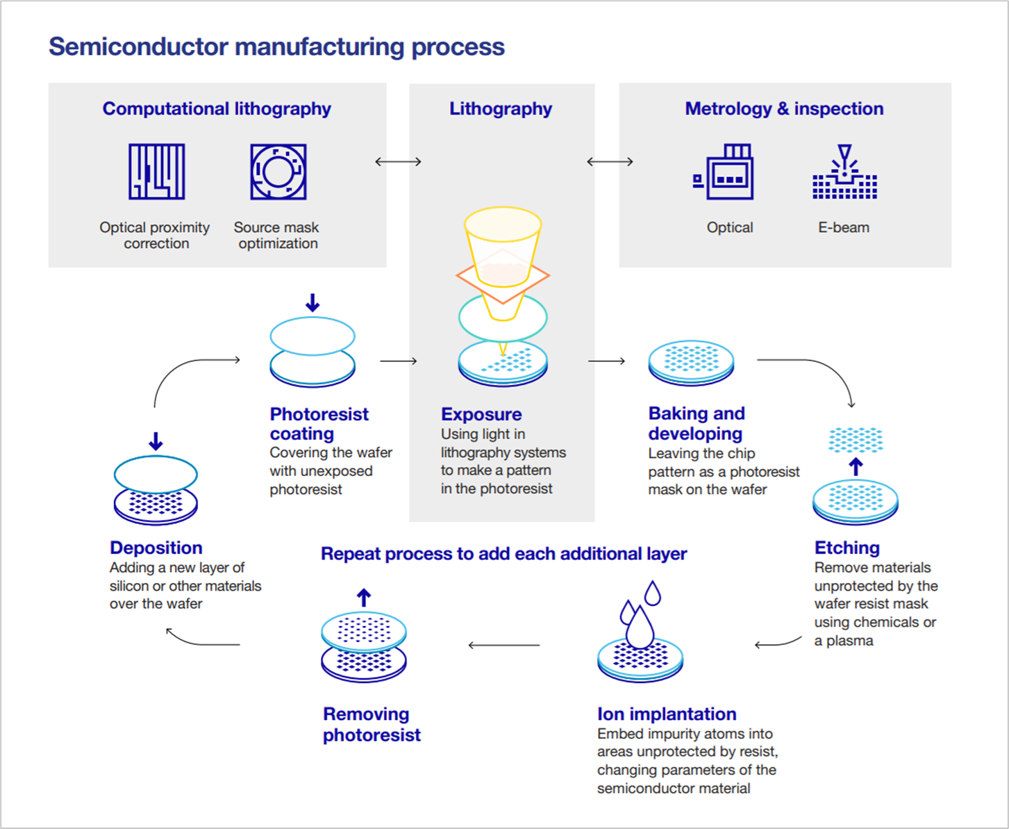
Source: ASML 2020 annual report
ASML’s revenue comes from the manufacture and sale of lithography systems and metrology & inspection systems. The company also generates revenue from providing management services for its installed base of lithography systems. Its customers are the world’s leading chip manufacturers and they include IDMs (integrated device manufacturers who design and manufacture chips) and foundries (contract manufacturers of chips for chip designers and distributors). The crown jewel in ASML’s portfolio of products is its EUV (extreme ultraviolet) lithography system. EUV lithography is currently the most advanced lithography process available and ASML is the only company in the world that has the technological knowledge to manufacture EUV lithography systems.
An important aspect of the lithography process is the critical dimension, the smallest structure that a lithography system can print. The critical dimension is determined partly by the wavelength of the light used – the smaller the wavelength, the smaller the transistors that can be printed. The EUV lithography process uses ultraviolet light with a wavelength of 13.5 nanometres (nm). Prior to the emergence of EUV lithography for high-volume chip manufacturing in 2017/2018, the state-of-the-art was a DUV (deep ultraviolet) lithography process involving light with a wavelength of 193 nm.
Just a few years ago, leading-edge chipmakers were already routinely using DUV lithography to produce chips containing structures with tiny geometries that are between 20 nm and 10 nm, sometimes even down to 7 nm (for perspective, a sheet of paper is about 100,000 nm thick). But as chipmakers pursued ever smaller geometries for chip structures (7 nm and below), they started running into cost and manufacturing issues associated with using DUV lithography for producing chips with such tiny features. The chipmakers realised that DUV lithography was approaching its limits. ASML once said that “if you were to write your name with a marker pen in increasingly smaller handwriting, you’d like to switch to a different kind of pen at some point, right?” DUV lithography had become a marker pen when chipmakers were looking for fineliners. This is where EUV lithography – with its use of light with a wavelength of 13.5 nm – comes into play.
An EUV lithography system is an engineering marvel. The system requires a vacuum chamber because EUV light is absorbed by everything, even air. Within the system, 50,000 tiny spherical tin droplets – each only 25 microns in diameter (for perspective, a human hair is about 70 microns thick) – are fired into the vacuum chamber every second. In the chamber, each tin droplet is then hit by two lasers and both lasers must hit each droplet with precision. The first laser changes the shape of a tin droplet from a sphere into something pancake-like; the second laser vaporises the pancaked droplet and turns it into plasma. This plasma in turn emits the desired EUV light with the wavelength of 13.5 nm. The EUV light that is created is then guided by a series of mirrors onto a silicon wafer to create a chip. The guidance of the EUV light needs to be incredibly precise – ASML describes it as “equivalent to shining a light torch from the earth and hitting a 50 eurocent coin placed on the moon.” The mirrors used in an EUV lithography system are so flat that if any of them were scaled to the size of Germany, there would be no bumps that are more than 0.1 centimetres high.
Each ASML EUV lithography system (a) requires floor space of around 80 square metres, or the equivalent of a small apartment, (b) contains 100,000 parts, 3,000 cables, 40,000 bolts, and two kilometers of hosing, (c) weighs around 180,000 kilograms, and (d) needs 40 freight containers, spread over 20 trucks and three cargo planes, to ship. In 2020, the average price of an EUV lithography system sold by ASML was €144 million, or around US$174 million.
Research on EUV lithography systems first started in the 1990s and ASML launched its own EUV development program 20 years ago in 2001. Early on, ASML’s customers expected the machines to be ready for commercial production by 2007, but the research & development process was fraught with difficulties. The company’s first primitive EUV prototype was launched in 2006 but a machine that is capable of high-volume chip manufacturing was ready only in 2017/2018, as mentioned earlier. Today, ASML’s customers are using the company’s EUV lithography systems in their factories for high-volume manufacturing of chips containing structures of 7 nm and below.
Given the complexities involved with the development and manufacture of EUV lithography systems, it’s perhaps not a surprise that there’s only one company in the world – ASML – capable of building such a machine.
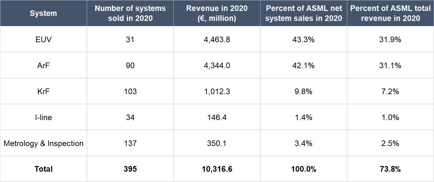
In 2020, ASML earned €13.98 billion in total revenue. This can be split into net system sales of €10.32 billion (73.8%) and net service and field option sales of €3.66 billion (26.2%). The latter category is essentially the management services that ASML provides for its installed base of lithography systems. ASML’s net system sales of €10.32 billion in 2020 can be segmented in a few ways.
One way is by looking at the chip markets that ASML’s systems are sold to. There are two types of chip markets: Logic, and Memory. Logic chips are for processing information in electronic devices while Memory chips are for storing large amounts of data in very small areas. In 2020, the Logic chips market accounted for €7.39 billion of ASML’s net system sales while the Memory chips market made up the rest at €2.92 billion.
Another way to segment ASML’s net system sales is by the type of systems that are sold. ASML has both EUV and DUV lithography systems in its portfolio. While EUV lithography is used for the most critical layers in a chip that contain the smallest transistors, DUV lithography systems are the current workhorses in the chip manufacturing industry and they are used for less critical layers that contain larger transistors. ASML has a number of DUV lithography systems that work with ultraviolet light of different wavelengths. The DUV systems are the ArF(Argon Fluoride) 193 nm system, the KrF (Krypton Fluoride) 248 nm system, and the i-line 365 nm system. As mentioned earlier, ASML also sells metrology & inspection systems alongside lithography systems. The following table shows ASML’s system sales in 2020 broken down by the type of system sold. The key takeaway is that EUV lithography systems is currently the most important system-category for ASML in terms of revenue, followed by DUV lithography systems.
Source: ASML 2020 annual report
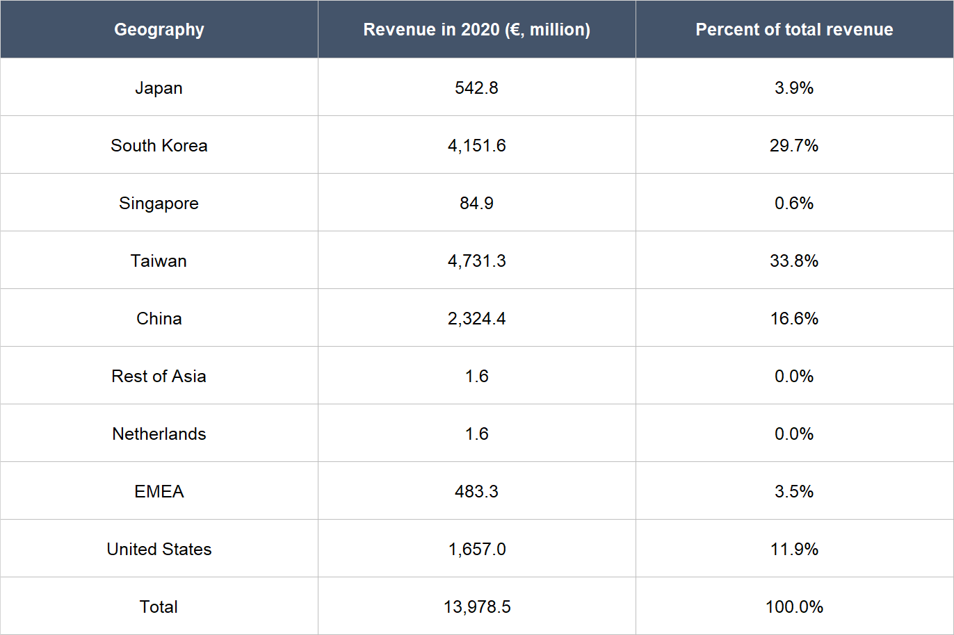
Here’s a table that shows a geographical breakdown of ASML’s revenue in 2020:
Source: ASML 2020 annual report
ASML is a geographically diversified company, but there’s still a significant amount of revenue that comes from South Korea and Taiwan. This is likely because the two geographies are the headquarters of Samsung and Taiwan Semiconductor Manufacturing Company (TSMC), respectively. The two companies are the second and third-largest largest chipmaking companies in the world based on their 2020 revenues (Intel, from the USA, is the first) and they are important to ASML. In 2012, to help defray costs and spread risk in its difficult journey to develop and commercialise EUV lithography, ASML invited Intel, Samsung, and TSMC to participate in a Customer Co-investment Programme. The trio took up ASML’s offer and invested a total of €5.23 billion (€1.38 billion for funding research into EUV lithography and other areas, and €3.85 billion for ASML shares) from 2012 to 2017.
Speaking of key customers, there’s significant customer-concentration at ASML and that’s a risk. In 2020, there were three customers that collectively accounted for 71.2% of ASML’s total revenue and each of them was more than 10%. Their identities are not revealed as far as we can tell. But we think they are likely to be Intel, Samsung, and TSMC, given what we know about their histories with ASML, and their status as three of the world’s largest semiconductor companies in the world.
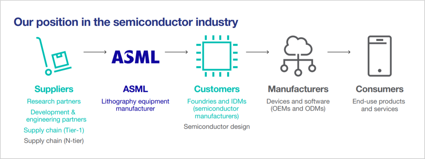
And to round up this description of ASML, the chart below is useful to understand where the company sits in the semiconductor industry:
Source: ASML 2020 annual report
Investment thesis
We have laid out our investment framework on Compounder Fund’s website. We will use the framework to describe our investment thesis for ASML.
1. Revenues that are small in relation to a large and/or growing market, or revenues that are large in a fast-growing market.
ASML’s future growth is backed by what we see as powerful tailwinds. Here’s how the company describes it in its latest annual report for 2020:
“Technology is evolving fast, and the next level of computing is dawning. The era of mobile computing – where you bring the computer with you – is evolving towards immersive ‘ubiquitous computing’, with computing power available wherever you go.
The transition to ubiquitous computing is enabled by what has been termed the ‘artificial intelligence of things’ (AIoT). AIoT is a smart and connected network of devices that seamlessly communicate over powerful 5G networks, allowing us to unleash the power of data better and faster than ever. This combination of artificial intelligence (AI) technologies with the internet of things (IoT) infrastructure will achieve more efficient IoT operations, improve human-to-machine interactions, and enhance data management and analytics. The potential of AIoT will gradually open up as IoT and AI increasingly intertwine, facilitated by 5G. The vast amount of data that people can access, and the insights this provides, will fuel semiconductor business growth and transformation.
There are around 40 billion connected devices currently in use, with more being added every second. This number is expected to increase to 350 billion devices by 2030. Connected IoT devices are expected to create up to 175 ZB (zettabyte) of data per year by 2025. In other words, one zettabyte (1021 byte) equals a trillion gigabytes, and to download 175 ZB data with average current internet connection speed would take one person 1.8 billion years. This big data will need to become fast data to allow for ubiquitous computing as we move towards ‘edge’ computing, where processing is brought as close to the source of data as possible, rather than in the cloud.”
Adding to the passages above are the following comments shared by ASML CEO Peter Wennink during the company’s earnings conference call for the first quarter of 2021:
“For the industry at a high level, we see three trends driving considerable growth this year and in the years to come:
The first trend, in the shorter term there is a more cyclical or “catch-up” driven demand from decisions made in 2020 due to the global pandemic. These shortages were initially evident in the automotive market but more recently there are also indications of supply tightness impacting other market segments. We expect this to drive considerable demand for lithography systems this year and into next year.
The second, is a secular growth trend driven by the digital transformation taking place as we become a more connected world, across both people and machines. This transformation was further accelerated over the past year with the increased remote activity and reliance on technology to stay connected. These secular trends are driven by expanding end market applications such as 5G, AI and High Performance Computing. These and other mobile, distributed applications drive demand for both advanced Logic as well as more mature technology required for the services and applications that drive the growth of the digital infrastructure. Along with increased Logic demand comes increased Memory demand. This in turn drives demand across our entire product portfolio.
And the third trend, which we are starting to see now and which we will likely continue to see longer term, is the desire for more technology sovereignty which includes semiconductor and silicon based technology, leading to a geographical decoupling as different governments put initiatives in place to localize supply chains and become more self-sufficient. This inevitably will create some level of inefficiency in the semiconductor supply chain and creates additional equipment demand as more fabs are strategically built across the globe.”
The passages above from ASML and Wennink underscore the underlying growth drivers across the globe for more chips, and also for more advanced chips. The table below, based on external market research cited by ASML in its 2020 annual report, shows the projected growth for various key markets of the semiconductor industry. From 2019 to 2024, the market opportunity for the entire semiconductor space is expected to rise by 7.3% annually to US$598 billion. For perspective, ASML’s revenue in the 12 months ended 31 March 2021 was €15.90 billion (around US$19 billion).
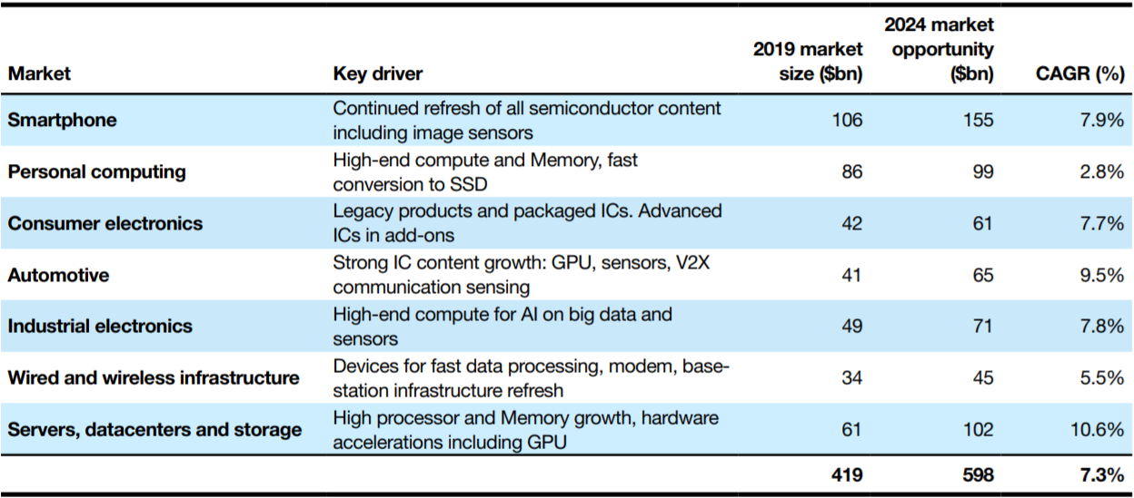
Source: ASML 2020 annual report
ASML’s view on the growth of the semiconductor industry is also backed up by Applied Materials, an American company that focuses on the manufacture and sale of equipment that are used to fabricate chips. The chart below, from Applied Materials, shows the significant growth in chip-content for a wide variety of electronics from 2015 to 2020 (actual) and then to 2025 (projected):
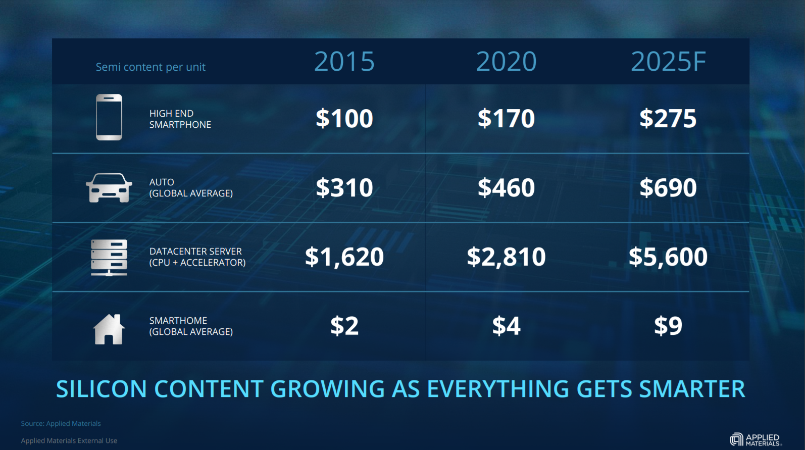
Source: Applied Materials 2021 investor presentation
We think that ASML is in a great position to ride on the rising demand for chips. The company has competitors in the lithography space, such as Canon and Nikon, who are both from Japan. But ASML is by far the most important player. According to a December 2020 report from Moody’s, a credit-ratings agency, ASML has a revenue-share of over 80% in the lithography market. And as we mentioned earlier, ASML is the only company in the world that knows how to manufacture EUV lithography systems, and these systems are crucial for chip manufacturers who are looking to create advanced chips with higher transistor-intensity per chip.
We’ve also seen ASML’s major customers pledge to invest heavily for their own growth in chip-production in recent times. For example, in 2019, Samsung said it would spend US$116 billion on capital expenditures by 2030. In another instance, Intel shared earlier this year in its Intel Unleashed: Engineering the Future press event that it will invest US$20 billion to build two chip manufacturing plants in Arizona in the USA. During the same press event, Intel also shared its plans to break into the foundry business at scale, with a focus on serving US and European chip designers. In yet another example, TSMC, the world’s largest contract chip maker, also announced earlier this year that it would invest US$100 billion over the next three years to increase its production capacity to meet rising demand. Given ASML’s stronghold over the lithography market, it’s likely that Intel, Samsung, and TSMC would have allocated meaningful amounts of capital within their aforementioned investment plans to the company’s EUV and DUV lithography systems.
(Intel’s move into the foundry space seems to be related to Wennink’s comments we shared earlier on countries – in this case, the USA – wanting more technology sovereignty. TSMC, based in Taiwan, controls more than 50% of the foundry market and many high-tech US companies such as Apple, Qualcoom, and Nvidia, depend on the company for advanced chips; Samsung and TSMC are currently the only foundries that are capable of manufacturing the most advanced chips of today, those that have structures with geometries of 5 nm.)
For its part, ASML continues to push the envelope. The company is developing its next generation of EUV lithography systems, known as High-NA, that could perform 70% better than its current EUV platform and enable the production of Logic chips with 2 nm structures and beyond. The abbreviation “NA” stands for “numerical aperture” and it is another factor that determines the critical dimension of a lithography system (we mentioned earlier that the critical dimension is the smallest structure that a lithography system can print). The NA indicates the entrance angle of light in a lithography system and if the lenses/mirrors used in the system come with a high NA, smaller structures can be printed. ASML’s customers have already ordered High-NA prototypes to evaluate high-volume production opportunities for a 2025 time frame.
2. A strong balance sheet with minimal or a reasonable amount of debt
ASML exited the first quarter of 2021 with €4.63 billion in total debt and €4.66 billion in cash and short-term investments. With slightly more cash and investments than debt, we think ASML’s balance sheet is in good shape.
It helps too that ASML has a long history of generating strong free cash flow, which is something we will discuss later.
3. A management team with integrity, capability, and an innovative mindset
On integrity
ASML is led by the 64 year-old Peter Wennink, who became CEO in 2013. Wennink joined ASML in January 1999 and was promoted in July of the same year to the chief financial officer role, a position which he held till he was handed the CEO hat. The other key leaders in ASML are shown in the table below.
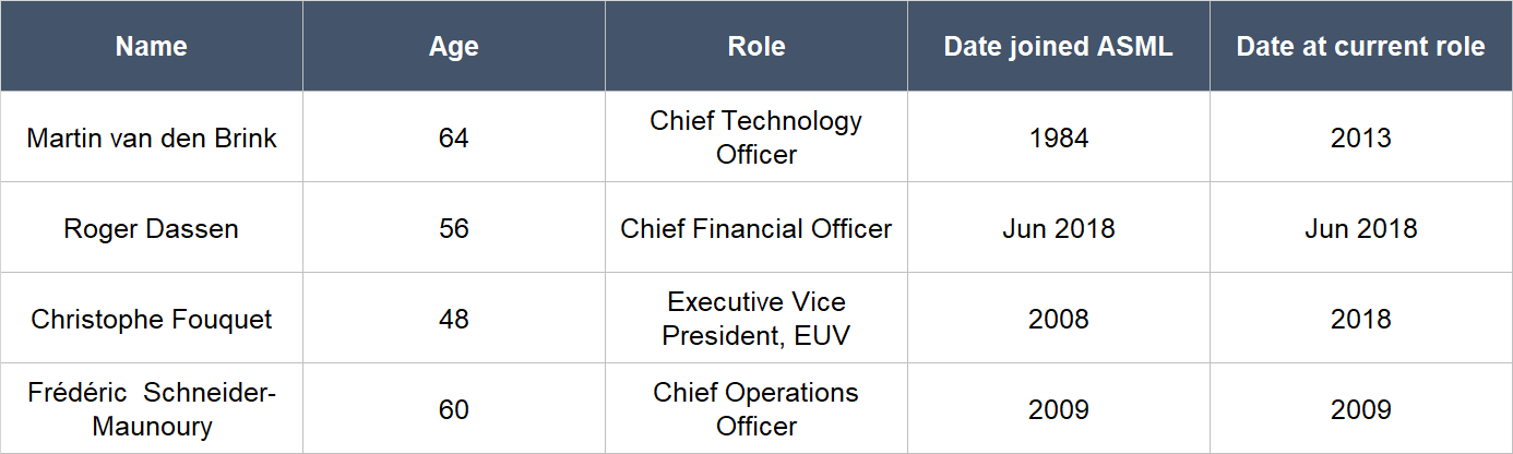
Source: ASML 2020 annual report
Most of ASML’s other key leaders, like Wennink, have been at the company for many years and some of them – like van den Brink and Fouquet – were promoted to their current roles. We appreciate the long tenures that ASML’s senior leadership have at the company. The fact that some of them were promoted to their current roles also speaks positively to ASML’s culture, in our view.
We think that ASML has a sensible compensation structure for its key leaders that demonstrates their integrity. The key points:
- Wennink’s base salary in 2020 was €1.02 million, a modest sum when compared to ASML’s net income and free cash flow of €3.55 billion and €3.63 billion, respectively, for the same year.
- For 2020, Wennink could earn a short-term cash incentive that has a target value of 80% of his base salary for the year. The actual value of the short-term incentive was determined by ASML’s performance for the year in the following areas: (1) Earnings before interest & tax margin; (2) gross margin for the sale of EUV lithography systems; (3) free cash flow; (4) level of progress along its product and technology roadmaps; and (5) market share, customer satisfaction, and product quality. Even though the measurement period for these areas is really short (just one year), we think good performances in them provide fuel for ASML’s long-term success. So Wennink’s short-term incentives are still aligned nicely with long-term shareholder value creation at ASML. Ultimately, Wennink’s short-term incentive for 2020 was 139.2% of the target value, or 111.4% (139.2% x 80%) of his base salary for the year.
- Wennink could also earn a long-term incentive for 2020, in the form of shares, that has a target value of 110% of his base salary for the year. The actual value of the long-term incentive would be determined by ASML’s performance over the three-year period from 2020 to 2022 in the following areas: (1) Its total shareholder return relative to the PHLX Semiconductor Sector Index, which comprises companies that are in the semiconductor industry; (2) return on average invested capital; (3) level of progress along its product and technology roadmaps; and (4) a broad array of ESG-related aspects, where ESG refers to environmental, social, and corporate governance. We think these areas all make sense, and we like the multi-year measurement period for them. We want to highlight the emphasis that is placed on ASML’s progress along its product and technology roadmaps (it partially determines both the short-term and long-term incentives that Wennink can earn) – we think this is smart, as ASML’s long-term economic value is closely tied to its ability to maintain technological leadership in lithography. Depending on how ASML performs in the four aforementioned areas from 2020 to 2022, the long-term incentive Wennink could earn ranges from 0% to 220% of his base salary for 2020.
- The compensation structures for the other key leaders of ASML that we introduced earlier – van den Brink, Dassen, Fouquet, and Schneider-Maunoury – all include modest base salaries, and short-term and long-term incentives with similar traits as Wennink’s.
We do note that there’s little skin in the game for ASML’s key leaders. As of 31 December 2020, Wennink, van den Brink, Dassen, Fouquet, Schneider-Maunoury, and Fritz van Hout collectively controlled just 102,260 ASML shares (excluding any unvested shares). At the company’s 4 May 2021 share price of US$629, their shares are worth ‘only’ US$64.3million. But this lack of meaningful ownership is nowhere near being a dealbreaker when we consider the well-crafted compensation structure for ASML’s management team. (van Hout was appointed as ASML’s chief strategy officer in 2018. He first joined ASML in 1984 – the year of the company’s founding – before leaving in 1993 and then returning to the company in 2001. He retired in April this year.)
On capability and ability to innovate
ASML’s ability to develop an EUV lithography system that is capable of being used for high-volume chip manufacturing – something no other company in the world currently can – and then successfully commercialise it, is shining proof that Wennink and his team are exceptional when it comes to execution and innovation. Adding another feather to their cap is the fact that they are not content to just coast along with ASML’s current generation of EUV lithography systems – as mentioned earlier, Wennink and his team are developing High-NA, the next generation of EUV lithography systems that can enable the production of Logic chips with 2 nm structures and beyond.
We want to highlight that Wennink and van den Brink both assumed their current respective roles of CEO and CTO in 2013. Back then, ASML was selling only a small handful of EUV lithography systems and was still some years away from developing one that could support high-volume chip manufacturing. It was only in 2017 when ASML’s sales of EUV lithography systems started ramping up. To us, this shows that Wennink, van den Brink, and the other current members of ASML’s senior leadership team deserve plenty of credit for the successful development and commercialisation of the company’s EUV lithography program. It’s also worth mentioning that even as Wennink and his colleagues were ramping up EUV lithography sales, they did not neglect the company’s installed base management services as well as the other lithography systems that are in the company’s portfolio – the second table below illustrates this (note the number of non-EUV lithography systems sold and the revenues they generate).
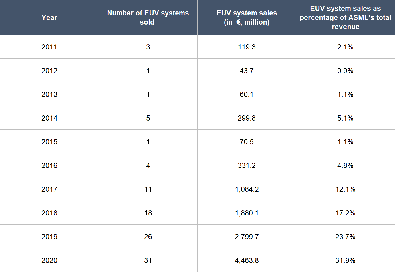
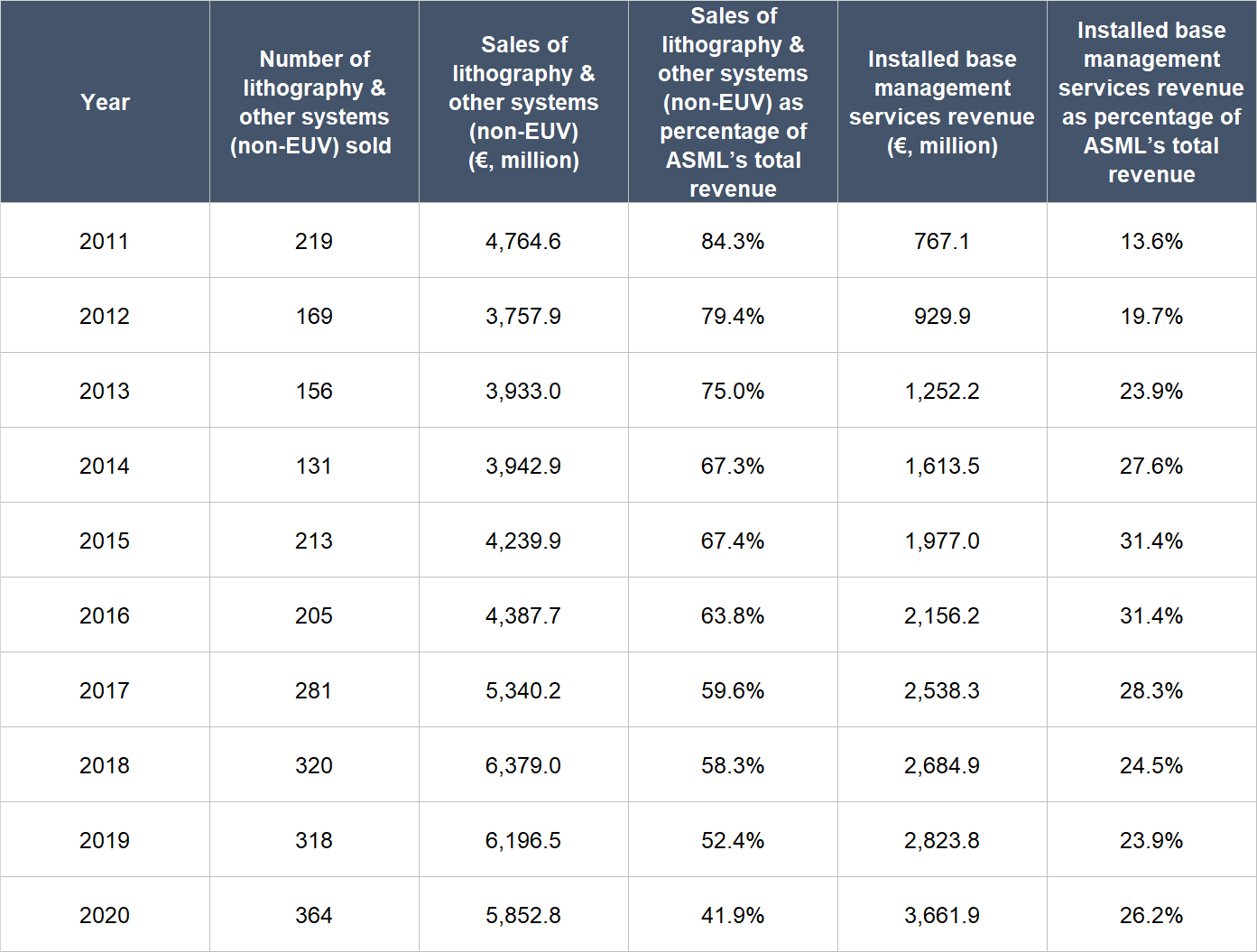
Source: ASML annual reports
We also want to highlight another thing about Wennink and van den Brink: They were already in senior leadership roles at ASML when the company first started developing its EUV technology in 2001, with Wennink being CFO (since 1999) and van den Brink being the head of ASML’s entire products & technology team (also since 1999). What this means is that both Wennink and van den Brink (especially van den Brink, since he was and still is leading products & technology) have had a massive say in ASML’s entire EUV lithography journey thus far. There are a number of aspects about this journey that we think shines a positive light on the foresight and smarts of the company’s leaders:
- When ASML first started conducting research on EUV lithography, there were other competing technologies that also held the potential to be the next-generation lithography platform that could help chip manufacturers massively shrink transistors. But ASML boldly chose to pursue only EUV lithography (and van den Brink likely had a huge hand in this, since he was the head of products & technology). Granted, the eventual positive outcome of ASML’s decision to go all-in on EUV lithography may have just been a lucky break. But we think ASML’s management still deserves credit for the perseverance and ingenuity they showed in overcoming the technical and financial challenges they faced in bringing the EUV lithography program to fruition.
- The perseverance can be seen in the time it took (nearly two decades!) for ASML to successfully develop a high-volume EUV lithography system. Earlier, we mentioned that ASML first started conducting research on EUV in 2001 and it was only in 2006 that a primitive prototype was shipped, in 2010 when the first R&D system was available, and around 2017 when the company’s EUV lithography systems could be used for mass chip production..
- As for the ingenuity, we shared earlier that ASML managed to get some of its key customers – Intel, Samsung, and TSMC – to provide funding for its research & development efforts for EUV lithography. We think this alone is already a laudable effort (and when the investments were struck, Wennink was CFO, so he likely had played a pivotal role in bringing the deals across the line). But there’s more – the results of the research that was funded by Intel, Samsung, and TSMC could be commercialised by ASML without any restrictions.
And speaking of co-funding research, this is something ASML is doing with at least one of its key suppliers, Carl Zeiss. Carl Zeiss supplies a number of the critical components – such as lenses, mirrors, and illuminators – in ASML’s EUV lithography systems. The EUV lithography process depends heavily on the precise guidance of the EUV light that is generated, and so the optical components within an EUV system, such as mirrors, have to be engineered to an extremely high quality. What Carl Zeiss is doing is no mean feat. In fact, ASML may have severe trouble in producing its lithography systems if Carl Zeiss has production difficulties or chooses to terminate its partnership with the company. In 2016, ASML agreed to fund a total of €760 million, over a six year period, for research that Carl Zeiss is conducting for ASML’s High-NA program; as of end-2020, the funding sum had been increased to a total of €1.35 billion. In 2017, ASML also acquired a 24.9% stake in Carl Zeiss for €1 billion. We think these are shrewd moves by Wennink and his team – they have managed to significantly lower the risk of Carl Zeiss becoming a stumbling block to ASML’s future growth.
In searching for investment opportunities, we have a soft spot for companies that have a fantastic workplace culture. This is something that Wennink and his team seem to have built successfully. ASML has excellent ratings on Glassdoor, a website that allows a company’s employees to rate it anonymously. ASML currently has a 4.1-star rating out of 5, 85% of ASML-raters would recommend a friend to work at the company, and Wennink has a 94% approval rating as CEO, far higher than the average Glassdoor CEO rating of 69% in 2019.
4. Revenue streams that are recurring in nature, either through contracts or customer-behaviour
Earlier, we shared that 73.8% of ASML’s revenue in 2020 came from the sale of systems. These are expensive systems – from millions of euros to more than €100 million each – and ASML sells relatively few of these. Indeed, as we already mentioned, ASML sold ‘just’ 395 systems in 2020. What these mean is that ASML’s revenue each year mostly revolves around the sale of relatively few expensive capital equipment. This is not what recurring revenues typically look like. But we are comforted by two things.
One, ASML has the rising demand for more chips and advanced chips as a long-term tailwind. With higher demand for chips comes more demand for the equipment to manufacture them. And as we’ve mentioned, the company’s key customers – Intel, Samsung, and TSMC – all have massive investment plans to expand their chip production capacity in the years ahead. With ASML’s dominance in the DUV lithography space, its complete monopoly over EUV lithography, and its drive to improve its portfolio of lithography systems, customers are likely to keep coming back to ASML to replace older systems or buy more machines.
Two, ASML does have recurring revenue. It comes from ASML’s installed base management services, which accounted for 26.2% of the company’s revenue in 2020. The revenue from installed base management services should also increase over time, driven by growth in ASML’s installed base, as well as an increasing contribution from EUV lithography systems as these systems run more silicon wafers in volume manufacturing.
5. A proven ability to grow
The table below shows ASML’s key financials from 2010 to 2020. We chose 2010 as the starting point because it was the year when ASML shipped its first EUV research & development system.
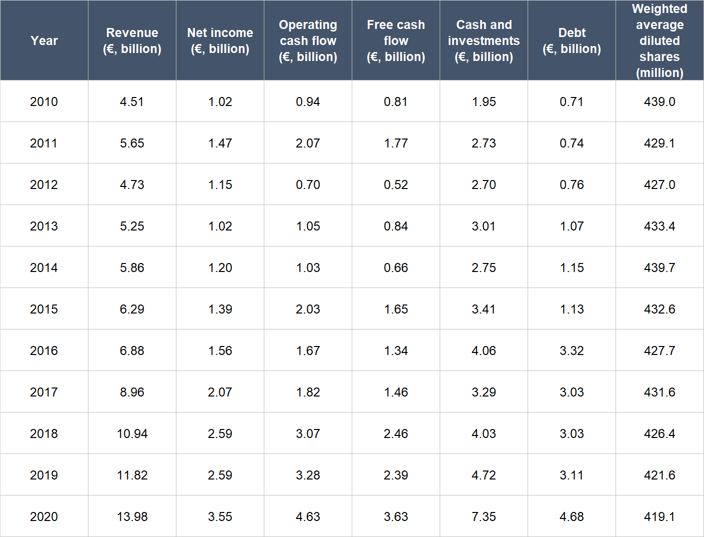
Source: ASML annual reports
A few important things to highlight from ASML’s historical financials:
- Revenue compounded at a respectable rate of 12.0% per year from 2010 to 2020. The annual growth rate accelerated to 17.3% for the 2015-2020 period, and came in at 18.3% in 2020.
- For 2010-2020, the compound annual growth rate (CAGR) for ASML’s net income was decent at 13.3%. For 2015-2020 and 2020, they accelerated to an excellent 20.7% and 37.1%, respectively.
- Operating cash flow was positive throughout the time period we are observing and had compounded at 17.3% per year from 2010 to 2020 and at 18.0% per year from 2015 to 2020. In 2020, operating cash flow was up by 41.2%. These performances are not too shabby at all!
- The dynamics for ASML’s free cash flow are similar to its operating cash flow. The financial number was positive for each year for 2010-2020 and the compound annual growth rate was 16.2%. The growth rate for 2015-2020 was slightly better at 17.0% per year while the performance in 2020 was fantastic with growth of 51.7%. We also want to highlight that ASML’s free cash flow margin (free cash flow as a percentage of revenue) was consistently strong: The averages for 2010-2020 and 2015-2020 were 19.9% and 21.8%, respectively.
- ASML’s balance sheet was strong throughout the time period we’re studying, with cash and investments outweighing total debt in each year.
- Dilution has not been a problem for ASML. The company’s weighted average diluted share count declined by 0.5% per year from 2010 to 2020, with most of the reduction coming in the recent years.
ASML posted impressive growth numbers for the first quarter of 2021, as illustrated in the table below. Revenue jumped by 78.8% while net income more than tripled. Even though operating cash flow and free cash flow were both negative in the quarter – and even deeper in the red compared to a year ago – we don’t think there’s anything to worry about. The free cash flow margin for the quarter actually improved from -34.7% to -26.1% and in recent years, ASML had been deriving most of its cash flows in the fourth quarter. We note that ASML’s growth in the first quarter of 2021 is skewed higher as the company lapped a relatively slow first quarter in 2020 because of the emergence of COVID-19. Nevertheless, ASML’s performance in the first quarter of 2021 was still impressive and the company has signalled for 30% overall growth for the year.
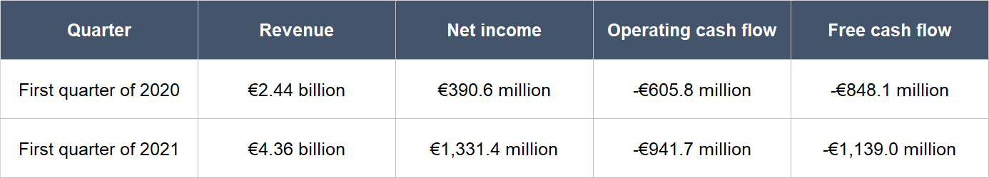
Source: ASML 2021 first quarter earnings update
6. A high likelihood of generating a strong and growing stream of free cash flow in the future
Over the past decade, ASML had produced a growing stream of free cash flow and achieved strong free cash flow margins, as mentioned earlier. With the tailwinds enjoyed by the entire semiconductor industry, and ASML’s position as the undisputed technological leader in lithography systems, the company looks set to continue growing its free cash flow in the years ahead.
We also want to highlight that ASML may be able to see an improvement in its gross margin (gross profit as a percentage of revenue) in the future. Currently, the gross profit margin of ASML’s EUV lithography systems is lower than the company-wide gross profit margin for the sale of lithography systems (49.9% in 2020). Meanwhile, the gross profit margin for the management services of the EUV installed base is also lower than ASML’s overall gross profit margin for installed base management (45.1% in 2020). ASML expects EUV systems to reach the company-wide gross profit margin in 2021 and also expects the EUV services gross margin to improve towards the company-wide level in the coming years. If ASML’s overall gross profit margin is higher in the future, that could lead to an even higher free cash flow margin. There’s already been a gradual improvement in ASML’s free cash flow margin since 2017, as illustrated in the table below, as the company’s EUV program matures.
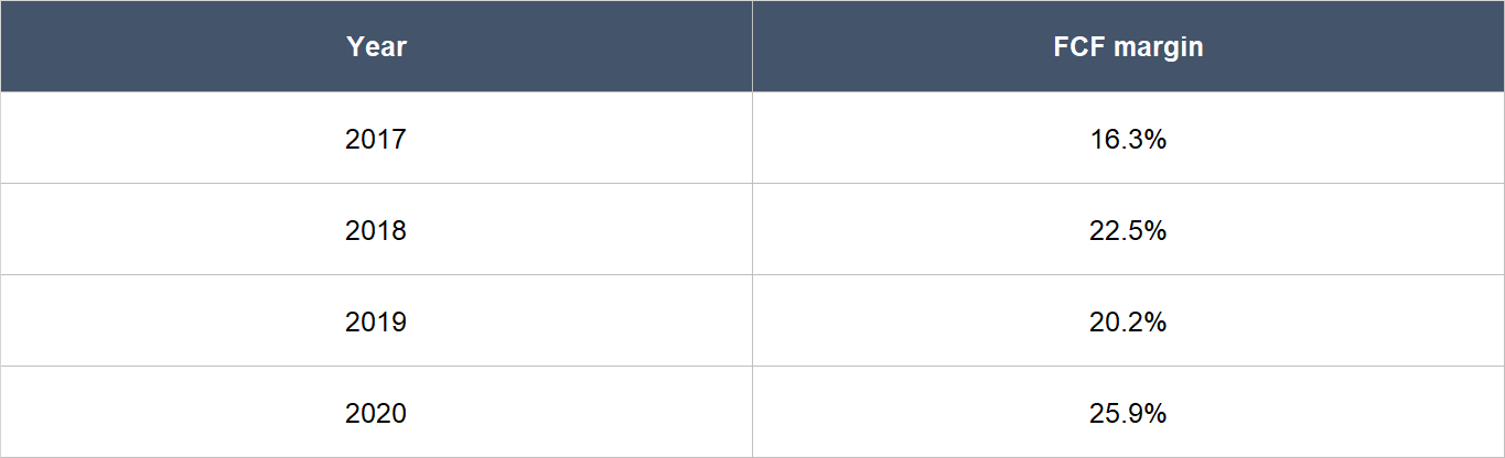
Source: ASML annual reports
Valuation
We completed our initial purchases of ASML shares in early April 2021. Our average purchase price was US$645 per share. At our average price and on the day we completed our purchases, ASML’s shares had a trailing price-to-free cash flow (P/FCF) ratio of around 63. We like to keep things simple in the valuation process. In ASML’s case, we think the P/FCF ratio is currently an appropriate metric to gauge the value of the company, since it has already been generating substantial free cash flow for a number of years.
The P/FCF ratio of 63 is high and that’s a risk. But we’re happy to pay up for ASML. This is because of the tailwinds we see in ASML’s business, and the monopoly position the company holds in EUV lithography, which is, again, a critical part of the world’s quest to produce ever more powerful chips.
For perspective, ASML carried a P/FCF ratio of around 65 at its 4 May 2021 share price of US$629.
The risks involved
There are a few risks that could derail our investment in ASML:
- A change of guard: We rate ASML’s current management team very highly. But CEO Peter Wennink and CTO Martin van den Brink are both already in their mid-60s and have been with the company for decades. Should either or both of them leave, ASML will have big shoes to fill and we’ll be watching the leadership transition.
- Concentration risk: Earlier, we discussed ASML’s customer-concentration and heavy reliance on Carl Zeiss – these are risks.
- A high valuation: We believe that ASML has massive growth opportunities and a high probability of being able to take advantage of the opportunities that it sees (after all, it does have a monopoly in EUV lithography). The company thus deserves its current premium valuation. But if there are any hiccups in ASML’s business – even if they are temporary – there could be a painful fall in the company’s share price. This is a risk we’re comfortable taking as long-term investors.
- Geopolitics: ASML is caught in the middle of the USA’s current tech war with China. China wants to build up its technological capabilities but the country needs lithography systems that can manufacture advanced chips. The USA however, has been blocking ASML from selling its EUV lithography machines to China. If tensions between the USA and China were to escalate from here, ASML’s business could suffer; in 2020, the company derived 16.6% of its revenue from China. Adding another layer of complexity to the geopolitical risk ASML is facing is the company having the Taiwan-based TSMC – the largest and most advanced contract chip maker in the world – as a key customer. Taiwan and China have long had a fraught relationship and China has made no secret that it sees Taiwan as its territory, even though Taiwan governs itself autonomously. If China were to invade Taiwan in the future – be it to seize TSMC for its technological knowledge, or simply because China wants unification – ASML could become a casualty.
- Obsolescence of lithography systems: For decades, chips that contain transistors have been the bedrock of computers as we know them – and ASML’s business has been growing on the back of the global demand for having more and more transistors per chip. But in recent years, researchers at companies such as IBM and Google have been building quantum computers with chips that are built very differently from the traditional transistor-based chip. In a well-publicised but somewhat controversial controlled experiment by Google in 2019, its quantum computer was shown to have significantly outperformed a state-of-the-art supercomputer that’s built with transistor-based chips. Should quantum computers with chips that are not based on transistors gain widespread adoption in the future, it could cause the obsolescence of transistor-based chips and ASML’s lithography systems. For now, quantum computing is still in its infancy and there’s also no widespread consensus yet on what’s the best way to build quantum computing chips (there’s been at least one successful experiment showing that quantum computing chips could possibly be built with traditional transistor-based chips). Nonetheless, we’re keeping an eye on things here because they represent a remote but existential risk to ASML’s business.
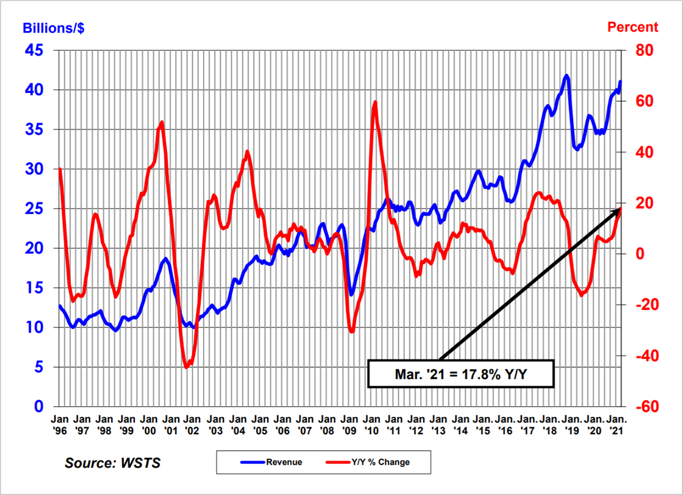
- Cyclicality in the semiconductor industry: Global semiconductor revenues have historically been cyclical even though there’s also been a clear long-term upward trend. These traits can be seen in the chart below, which shows monthly global semiconductor revenues (the blue line) and their year-on-year growth rates (the red line). Our eyes are focused on the long-term growth in the semiconductor space, but if there’s a long cyclical winter in semiconductor revenues in the future, ASML’s business could also catch a prolonged cold.
Source: Semiconductor Industry Association
Summary and allocation commentary
To sum up, ASML has:
- A huge and growing opportunity in the lithography market, and an enviable monopoly over the most advanced lithography platform currently, EUV lithography
- A robust balance sheet with more cash and investments than debt
- A management team with (1) a well-designed compensation structure that demonstrates integrity, and (2) an excellent long-term history of execution and innovation
- Customers that likely will keep coming back for more
- A long track record of growth in revenue, net profit, and free cash flow
- A high likelihood of producing a growing stream of free cash flow in the future
There are risks to note, such as key-man risk; a high-level of customer concentration; a heavy reliance on one supplier; a high valuation; exposure to geopolitics involving the USA, China, and Taiwan; the chance that lithography systems could become obsolete in a future where non-transistor-based computing chips become widely adopted; and the possibility that there could be a prolonged downcycle in the semiconductor industry in the future.
After considering the pros and cons, we decided to initiate a position of around 1.5% in ASML in April 2021. We appreciate all the strengths we see in ASML’s business, but our enthusiasm is tempered by the company’s high valuation.
And here’s an important disclaimer: None of the information or analysis presented is intended to form the basis for any offer or recommendation; they are merely our thoughts that we want to share. Of all the other companies mentioned in this article, Compounder Fund also owns shares in Alphabet (parent of Google) and Apple. Holdings are subject to change at any time.